1. Introduction
In the world of modern computing, where artificial intelligence, data centers, and high-performance gaming demand faster and more efficient systems, High Bandwidth Memory (HBM) has emerged as a revolutionary technology. But as this technology evolves, so does its packaging approach. Over time, the industry has witnessed a phenomenon known as HBM packaging technology divergence—a branching out of packaging methods tailored for different needs.
This guide provides a clear and detailed explanation of what “HBM packaging technology divergence explained” really means, how it came to be, the different forms it has taken, and where it’s headed next.
2. Fundamentals of HBM Packaging
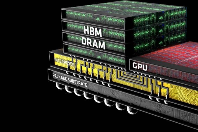
High Bandwidth Memory is a type of RAM designed to provide extremely fast data transfer between memory and processors. Unlike traditional DRAM modules that sit separately on a motherboard, HBM stacks memory chips vertically and connects them using Through-Silicon Vias (TSVs). This stacking reduces space requirements while delivering significantly higher bandwidth.
The evolution of HBM has been rapid:
| Generation | Bandwidth per Pin | Total Bandwidth per Stack | Max Stack Height | Common Use Cases |
|---|---|---|---|---|
| HBM | ~1 Gbps | Up to 128 GB/s | 4–8 dies | Early HPC, GPUs |
| HBM2 | 2 Gbps | 256 GB/s | 8 dies | HPC, AI, graphics |
| HBM2E | 3.2 Gbps | 460 GB/s | 8–12 dies | AI training, servers |
| HBM3 | 6.4 Gbps | 819 GB/s | 8–12 dies | Advanced AI, HPC |
| HBM3E | 9.2–9.8 Gbps | Over 1 TB/s | 12 dies | AI, supercomputers |
3. What Does “Divergence” Mean in HBM Packaging?
When we talk about HBM packaging technology divergence, we’re referring to the way this technology has split into different packaging methods to meet unique needs in various markets.
Originally, HBM used a uniform design—stacked DRAM dies connected to processors via silicon interposers. But as markets demanded different combinations of performance, cost-efficiency, and energy savings, manufacturers started experimenting with multiple packaging strategies.
Divergence happens because:
- Performance demands differ – AI supercomputers need maximum speed, while mobile devices require efficiency.
- Manufacturing costs matter – Not every device can justify premium interposer-based designs.
- Thermal and power challenges – Dense stacking creates heat issues that some designs must address differently.
4. Variants Along Divergent Paths
The divergence in HBM packaging has created several distinct variants, each optimized for a particular set of goals.
- HBM2 / HBM2E – Proven and cost-effective, widely used in professional GPUs and AI inference chips.
- HBM3 / HBM3E – Designed for extreme performance in AI training and HPC clusters, offering the fastest bandwidth available.
- HBM Lite – A streamlined, lower-layer version intended for mid-range devices where full-stack performance isn’t necessary.
- Interposer-less HBM – Uses advanced connections without a costly silicon interposer, reducing manufacturing cost.
| Variant | Main Focus | Pros | Cons |
|---|---|---|---|
| HBM2 / HBM2E | Balanced performance | Mature tech, lower cost | Lower bandwidth than newer versions |
| HBM3 / HBM3E | Extreme speed | Highest bandwidth for AI/HPC | Highest cost, complex manufacturing |
| HBM Lite | Affordability | Lower cost, easier integration | Reduced capacity and bandwidth |
| Interposer-less | Cost reduction | Cheaper to produce, simpler design | May limit bandwidth potential |
5. Technical Drivers of Divergence
Several technical factors push HBM packaging into different directions:
- TSV Advancements – Improvements in TSV manufacturing have enabled taller stacks and faster interconnects, but costs remain high.
- Interposer Technology – Traditional HBM relies on large silicon interposers, but alternatives like organic substrates and bridge chips are emerging to reduce costs.
- Thermal Design Needs – High-density memory generates heat, so packaging must adapt with better heat spreaders, underfill materials, and cooling solutions.
6. Advantages and Trade-offs
Divergence is not just about innovation—it’s about strategic choices.
Advantages:
- Tailored performance – Manufacturers can select the right HBM variant for the job.
- Cost flexibility – Not all systems need the most expensive memory configuration.
- Energy efficiency – Some variants focus on lower power draw.
Trade-offs:
- Complexity in design – More variants mean harder integration for system designers.
- Fragmentation risk – Too many formats can create compatibility challenges.
- R&D costs – Developing multiple approaches raises investment needs.
7. Industry Trends and Competitive Dynamics
The HBM market is now highly competitive, with SK hynix, Samsung, and Micron leading innovation. For example, SK hynix is currently the primary supplier for NVIDIA’s AI chips using HBM3, while Samsung is investing heavily in HBM3E production.
China’s memory industry is also catching up, with companies like CXMT working on their own HBM versions to reduce dependency on imports.
8. Future Trajectories
The next generation—HBM4—is expected to break new records in bandwidth and capacity, possibly exceeding 1.5 TB/s per stack. Hybrid bonding and improved packaging integration will make it easier to merge compute and memory into single advanced modules, reducing latency further.
We may also see more convergence between compute and memory packaging, where processors and HBM are co-packaged to create AI accelerators with unmatched efficiency.
9. Conclusion
When you see the phrase “HBM packaging technology divergence explained”, it’s about understanding how a single memory technology has split into multiple specialized paths to serve different industries and goals. From ultra-high-bandwidth AI accelerators to cost-efficient mid-tier GPUs, HBM’s packaging diversity ensures it will remain a central pillar of computing innovation for years to come.
Other Articles
Guangzhou Xinhe Packing Technology Manufacturing AliExpress
Checkpoint Exam: Emerging Network Technologies Exam


Leave a Reply